| Log In | Not a Member? |
Support
|
|
G5 Performance ProgrammingOverview The PowerPC 970 (G5) is largely similar to previous PowerPC processors in the sense that all of the previous good practices apply. These include enabling full compiler optimizations, loop unrolling, function call inlining, proper alignment of data, attention to pipeline latencies, dispatch limitations, etc. As always, the largest opportunities for performance improvement comes from high level optimization techniques, most importantly choosing the right algorithm. Once you have selected the right algorithm and done all important high level tuning, then the usual collection of techniques common to achieving peak G4 performance are applicable to the G5. There are some key differences between the G4 architecture and the G5, however, that can dramatically affect how you approach solving low level code tuning problems. Developers should be familiar with the general tuning advice for G5 offered in these two documents: In addition, beyond these pages, the best source of PowerPC 970 tuning advice and architectural documentation is likely to be the Power4 Tuning Guide. This is because the Power4 and PowerPC 970 have nearly identical scalar cores. The addition of a AltiVec (VMX) unit is the largest difference. We will spend most of our time talking about that here. This page is intended to be an addendum to the above sources with information specifically relevant to tuning for AltiVec and high performance programming in general. It is targeted towards the segment of the developer population that is already knowledgeable about high performance programming and using AltiVec on the G4 processor family. NEW! — IBM has released some additional information about the PowerPC 970fx (G5), including a PowerPC 970fx User Manual. The User Manual should contain the most up to date and accurate description of the G5 and should be your primary source of reference. (January 20, 2005) OverviewIt is expected that developers will find that the G5 delivers a large step up for AltiVec performance. Memory bandwidth on the G5 is greatly enhanced over its predecessors. This will greatly improve code performance on code operating on uncached data. For data in cache, the G5 provides twice the number of load/store units of previous PowerPC processors. Since most AltiVec code is limted by load / store performance, many vectorized applications will see large immediate performance gains on G5. These will solidify as further attention is given to tuning for the new architecture. In our experience, tuning for the G5 more often than not results in a performance improvement for G4, so tuning your code to be responsive to the needs of the G5 is often an all around win. Beyond two LSUs, parallelism in the G5 core is greatly enhanced in a number of other ways. Up to 4 instructions plus one branch may be dispatched per cycle, up from three per cycle on the 7450. Most pipelines are longer on the G5 as well. Finally, there are dual scalar floating point units for top floating point performance. With all this added parallelism, up to 200 instructions can be in flight simultaneously in the G5 core, compared to a few dozen on the G4. The G5 aggressively reorders the execution of instructions much more so than the G4 did. This is accomplished through the use of reordering issue queues. This can complicate your understanding of instruction flow through the machine. Apple has made available a PowerPC 970 cycle accurate simulator as part of the CHUD 3.0 performance tools package to help you understand better how your code is performing on the new architecture. Instruction Level Differences Between G4 and G5
The AltiVec core itself is most similar to the PowerPC 7400, with similar dispatch limitations into the permute and VALU units. A few AltiVec instructions behave slightly differently between G4 and G5. These differences are within the bounds of the AltiVec specification and generally lie in the realm of undefined behavior.
vec_ldeWhen vec_lde (vector load element) is used, the contents of the other elements in the vector are undefined. The G4 zeros the unused elements. The G5 treats the instruction as a lvx, meaning that the data in the other elements are drawn from the surrounding data as it appears in memory.
Please note that the behavior of vec_lde continues to be undefined for elements other than the one that is loaded, and the implementation may change again in the future. vec_sll and vec_srlThe AltiVec PEM requires that the number of bytes/bits for the shift be splatted across all bytes of the vector containing the number of bytes/bits to shift. Some previous G4 models did not enforce this restriction. (The Motorola AltiVec PIM pictures are also a bit misleading in this regard.) The G5 requires that the shift count be splatted across all bytes of the shift mask, otherwise behavior is undefined. The shift left or right by octet variants on these instructions do not have this restriction. vec_dstThe streaming prefetch instructions should be used with care on the G5. DST's are serializing and may introduce an approximately 10 cycle bubble in your program execution each time they are used. They can have detrimental effects when used in the inner loop in some functions. Since the typical usage pattern for vec_dst can still be used to good effect on G5. It works best for medium sized data segments less than 4K in size and large enough that it is more efficient than a few vec_ldl and vec_stlLRU loads and stores are treated as regular loads and stores.
|
| fres: |
mean error
|
max error
|
|
PPC750:
|
1/15848.4
|
1/5256.11
|
|
PPC7450:
|
1/5462.39
|
1/2049
|
|
PPC970:
|
1/669.415
|
1/256
|
Likewise, the frsqrte instruction is supposed to have no more than one part in 32 error. Some earlier processors were more accurate than that.
frsqrte:
If you previously did not verify that your use of fres and frsqrte would tolerate the allowable error bounds provided by the PowerPC specification, it is possible your code is misbehaving on G5. Please note that not all processors in a class necessarily have the same precision. For example, not all G3s provide better than 12 bit accuracy for fres and frsqrte.
How accurate is your processor? Find out!
Overview of Instruction Flow Through the G5
The way the G5 handles instructions in its core is fundamentally different than the way a G4 does it in a number of respects. Some discussion of the execution pathway is therefore warranted. For comparison, a discussion of the 7400 execution model is to be found in the Performance Measurement section and the 7400 and 7450 User Manuals. The chief differences arise from the fact that the G5 may crack or microcode instructions, while the G4 does not. Also the G5 groups instructions into dispatch groups that dispatch and complete together. There are a number of complicating factors associated with what instructions may and may not group together. Finally, the G5 has reorder queues in front of the execution units that allows the G5 to execute instructions even more out of order than the G4 does. The G5 has dual load/store units and dual floating point units. This can result in a profound performance improvement for many code samples.
Fetch
Instructions enter the G5 in fetch blocks of 8 instructions aligned to 32 bytes and placed in an instruction fetch buffer. The instruction fetch buffer can hold 32 instructions. While this is not especially unusual, what happens from this point forward is a significant departure from G4. The processor reads through these in order, biting off up to five instructions to form a dispatch group each cycle. The instructions in the dispatch group will stay together as a group until they are retired, returning all their renames to the free pool and releasing any other resources as a set, unless an error is detected. Because of this instruction grouping, the core of the G5 is somewhat VLIW-like.
The dispatch groups can be up to five instructions in size, consisting of up to four non-branch instructions plus one optional branch instruction, appearing in the order that they appear in the instruction stream. The branch, if present, always terminates a dispatch group.
Example: if the instruction sequence starts with two non-branch instructions followed by a branch and then two more non-branch instructions, the processor will form a three instruction dispatch group out of the first two non-branch instructions and the branch. The next two non-branch instructions will form part of the next dispatch group. Each cycle, one dispatch group can be dispatched.
A dispatch group may also be terminated early if any of the following conditions is true:
- The instruction fetch buffer does not contain any more instructions or if too many condition register modifying instructions appear in the dispatch group
- A microcoded instruction appears
- An instruction appears that modifies a unrenamed special purpose register.
Certain dependencies are not allowed within a group. For example, if a load and store in the same group are to the same address (or to addresses with the same lower 16 bits), then it is not correct to execute them concurrently, since the aliasing order might not be correct. When the processor encounters this situation, it aborts processing the instructions and breaks the dispatch group apart, and executes the instructions individually. Unfortunately, the processor can't know whether this has happen until the effective address is calculated for both, which happens near the end of execution. This abort/retry process is very expensive, since it amounts to a pipeline flush. It is seen most frequently in processes that move data from one register file to another wherein there are data size changes, such as int to float conversions. Recent versions of GCC-3.3 and later can detect and avoid this pattern. Shark will also automatically detect this pattern.
Decode
The G5 does instruction cracking and microcoding. A number of PowerPC instructions are divided up into two or more internal instructions called microoperations (µops). Those that are broken into two are said to be cracked. Such instructions take up two spaces in the dispatch group. Those that are broken into three or more are said to be microcoded, and take up an entire dispatch group unto themselves. No AltiVec instructions are cracked or microcoded, though vector stores have a vector and LSU component that is visible in the simulator. These only take up one slot in the dispatch group, but take up two issue queue slots as per other stores — one in the LSU and one in the vector store unit.
Cracked and microcoded instructions are typically LSU and integer operations. Most notably, the update indexed forms of the various load and store instructions may be microcoded. Their use is therefore discouraged for performance reasons. Most dot forms of instructions are cracked or microcoded. In addition, misaligned loads and stores may be microcoded. Here is a list of cracked and microcoded instructions (tags inactive mode). The good news is that some misaligned floating point LSU operations, while microcoded, are at least handled in hardware.
Dispatch
Once a dispatch group is formed, it enters the dispatch phase during which processor resources are gathered to make sure it has everything it needs for all the instructions to execute to completion. There must be at least four spaces available in the store reorder queue (SRQ) in case all four non-branch instructions are stores, and an appropriate number of entries in the load reorder queue (LRQ) for any loads.
In addition, each instruction in the group that returns a result must be assigned a register to hold the result. The G5 has eighty 128-bit vector registers. At any given time, 32 of these are devoted to serve as the 32 architected AltiVec registers. The other 48 are available as rename registers for allocation in the dispatch phase.
When the various resources required to execute the instructions in the dispatch group are gathered, the instructions are dispatched to various issue queues to await their operands to appear so that they can begin execution. Each issue queue feeds into an execution unit. There is one for the VALU, one for the vector permute unit, one for the branch unit, one for CR, and two each for the dual FPUs and LSU/FXUs. (The LSUs and FXUs share a pair of issue queues.) Up to four instructions can go into each family of issue queues for most execution units. It is possible to dispatch four vector floating point unit instructions per cycle into the VALU queue, for example. Any combination of these is of course allowed, e.g. two loads, a permute and a VALU instruction can be dispatched in a cycle. Only one branch per cycle can be issued because only one branch is allowed in a dispatch group. Only two CR modifying instructions are allowed per cycle.
Where there is more than one execution unit capable of performing a given task, (there are two FPUs, two LSUs and two pseudo-symmetric integer units), then each execution unit has its own queue. Which queue the instruction goes into depends on its position in the dispatch group. Instructions at position 0 and 3 in the dispatch group go into the queue for execution unit 0. Instructions at position 1 and 2 in the dispatch group go into the queue for execution unit 1. (See illustration of data flow through the FPU as an example.) Thus, instruction ordering can be at times important, since certain patterns may result in all instructions of a certain type going to just one of the two execution units. An instruction can be dispatched into the VALU and VPERM queues from any and all slots in the dispatch group, except the optional fifth slot dedicated to branch instructions.
In order to determine where an instruction appears in the dispatch group, one must know the alignment of the dispatch groups. Dispatch groups start at a branch target address, and generally happen every four instructions for branchless code after that, except when one of the other hazards described above happens. You can recognize dispatch groups in the Shark assembly view as strided samples that appear every four instructions or so, with no samples in between. This happens because samples are attributed to the first instruction in a dispatch group. Shark also has a static simulator feature that does a reasonably good job of predicting them. They can also be seen with more accuracy in the cycle accurate PowerPC 970 simulator in CHUD 3.0.1 or later.
Note that in the context of a loop, dispatch groups may appear in one "phase" the first time through the loop and then appear in a different phase starting at the top of the loop for successive iterations. Typically this will be seen as a set of bright samples every four instructions and another set of weak ones every four instructions.
The decode and dispatch process takes 6 cycles.
Issue
The issue queues feed directly into the execution units. Each cycle one instruction will be moved from each issue queue into its corresponding execution unit, provided that there is an instruction for which all the data dependencies are resolved. The instructions do not flow through the queues in a first-in first-out manner. This is a departure from G4, where instructions within a certain execution unit would execute in the order they appear in the instruction stream. Instead the G5 can reorder within the context of the queue. Usually it tries to execute the oldest instructions first, but if an old one is blocked because the input operands are not ready yet, another item in the issue queue will execute first instead. The number of instructions that can fit in the queues are as follows:
Unit |
Queue
Size |
|
| FPU1 |
10
|
|
| FPU2 |
10
|
|
| LSU1 / IU1 |
18
|
|
| LSU2 / IU2 |
18
|
|
| branch unit |
12
|
|
| condition register |
10
|
|
| VPERM |
16
|
|
| VALU |
20
|
The integer and load/store units share a issue queue. The integer/load/store queue can issue two instructions per cycle — one to an integer unit and one to a load/store unit. Since there are two such queues, 2 integer and 2 LSU operations can be issued per cycle.
The queues provide buffering capacity that will help more efficiently deal with data dependency stalls. In certain cases involving very small loops, the issue queues can have the effect of automatically unrolling loops for better pipeline usage. In extreme cases, this might be used as a strategy to save registers if 32 registers are not enough to saturate the pipelines with your algorithm, though generally speaking, the issue queues are not large enough for this to work with most unrolled AltiVec code, nor are there necessarily enough rename registers to support this technique. Some care is required as it would also require that you schedule code with lots of serial data dependencies that would execute quite poorly on processors without reordering issue queues such as the G4.
The queues consume rename registers. This happens because the rename registers are allocated in the dispatch phase before the instructions enter the issue queue. Instructions waiting to execute in the issue queues therefore tie up processor resources without doing work. For vector code, up to 36 of these can be sitting in the LSU issue queues for stalled loads. Another 36 can be in the VPERM and VALU issue queues for stalled vector instructions. Finally, renames are required for instructions that are currently executing or waiting to retire because other instructions in their instruction group have not finished executing. (The LRQ has 32 entries, and 80 vector instructions can be in flight before we run out of dispatch groups, so this number is actually somewhat smaller.) As a result, it remains important for you to schedule your code carefully to avoid having a lot of stalled instructions sitting in issue queues on G5, even with an aggressive code reordering facility to back you up.
Execution
Once the instructions enter the execution unit pipelines, they move through in the usual fashion. Up to 10 instructions can enter execution each cycle: 2 LSU, 2 FXU, 2 FPU, 1 VPERM, 1 VALU, 1 CR and 1 branch. The pipeline lengths are as follows:
| Execution Unit: |
cycles
|
|
| IU (+, -, logical, shift) |
2-3
|
|
| IU (multiplication) |
5-7
|
|
| FPU (+, -, *, MAF) |
6
|
|
| LSU (L1 hit) to GPR, FPR, VR |
3,5,4-5
|
|
| LSU (L2 hit, loads only) |
11
|
|
| VPERM |
2
|
|
| VSIU (part of VALU) |
2
|
|
| VCIU (part of VALU) |
5
|
|
| VFPU (part of VALU) |
8
|
Latencies presented are from empirical measurements for back to back serially dependent operations, except LSU operations.
The permute unit and VALU each maintain their own copies of the vector register file, which are synchronized on the half cycle. This adds one cycle of latency when a VALU result is used by a permute operation or a permute result is used for a VALU operation.
These pipelines are longer than what you will find in a G4. For code to scale with processor frequency on a G5, it is often necessary to unroll loops more than what is normal for a G4. It is recommended that you unroll all code to a depth of at least 8, so that 8 independent instructions can occupy the pipelines concurrently. This will help avoid pipeline bubbles and make sure you use the processor to its fullest potential. Future processors are likely to have even longer pipelines. More unrolling will help make sure that your code scales with new processors as they are released.
Completion
When all instructions from a dispatch group have finished executing, the dispatch group can be retired. The rename registers and other resources that it used will be returned to the free pools. Up to 20 dispatch groups can be in flight concurrently. Dispatch groups must be retired in the order that they are created. One dispatch group may be retired per cycle.
The Caches
Architecture
The level 1 data cache is 32kB and 2 way set-associative. The unified level 2 cache is 512kB and 8-way set associative. In comparison, the more recent G4s have a 256kb L2 cache. The PowerPC 7457 (used in the newer aluminum powerbooks) has 512kB cache. The data coherency point on the G5 is the L2 cache, rather than the L1. For this reason, stores are always sent to the L2 cache in addition to the L1 cache.
The G5 has no L3 cache, so the amount of space available to use in the cache hierarchy may be reduced on the G5 compared to some G4 systems. The G4 supports up to 2 MB of L3 cache.
Developers should be cautioned that a 512kb chunk of data that is contiguous in the virtual address space is not likely to fit in a 512kb L2 cache on any PowerPC. This is because the cache is physically mapped and the set of physical pages used to service a set of contiguous virtual pages are not themselves likely to be contiguous. (Read More.) As always, experimental determination of the best tile size to break your problem set into is required.
Throughput
Front side bus performance is dramatically improved on a G5 compared to the G4. To illustrate, let's do a small throughput comparison between G4 and G5. We are going to be totally unfair in this comparison. We will compare L1 to register throughput on a G4 against front side bus performance on a G5. Normally on any computer, we'd expect that the L1 to register throughput would be many times greater than its front side bus performance. Looking at the most common data size, a 32 bit integer load or store on a G4, we find that we can do one of these per cycle on a G4. On a 1.4 GHz G4, this means we can do:
4 byte load or store per cycle * 1.4e9 cycles/second = 5.6e9 bytes / second
This corresponds to about 5.3 GB/s for data throughput between the L1 cache and register. Of course, that is only in one direction, load or store. If you intend to copy data — an operation that involves both loading and storing — then the peak theoretical throughput is cut in half to about 2.67 GB/s, for data copies in the L1 cache. Most functions load and store data, so this is a probably a better thing to look at.
In comparison, the G5 front side bus (the data path between the memory controller and the processor) on a 2 GHz G5 operates at 1 GHz and can transfer 4 bytes per beat in each direction. There is some transactional overhead in this process, so the maximum throughput is 3.2 GB/s in each direction, rather than a full 3.8 GB/s (4e9 bytes/s). Traffic between memory controller and DRAM has a peak theoretical throughput of 6.4 GB/s. The read and write busses are independent, so aggregate throughput (copies must do both) is actually twice that. This gives us a peak theoretical throughput of roughly 6.4 GB/s. However, for copy operations we need to look at the throughput of the entire copy, so 3.2 GB/s is the right number to look at.
Therefore, peak theoretical front side bus throughput for RAM to RAM copies on a G5 is faster than L1 to L1 copies on the fastest G4 when the G5 was released!
For completeness, the L1 to register throughput on a 2.0 GHz G5 for 32 bit ints is:
(4 byte load + 4 byte store per cycle) * 2.0e9 cycles/second = 16.0e9 bytes/second
The G5 has two load store units, so it can move two 32 bit words per cycle rather than one. (Two loads per cycle are also possible. Two stores per cycle are not possible.) Of course, this discussion is complicated by the fact that the G5 has 64-bit integer registers and both machines have AltiVec (128 bit registers). Floating point stores on recent G4's (PPC745x) are not pipelined and so were not considered for this discussion. Store throughput is much slower on the G4 compared to G5.
Latency
Of course, throughput is only half the story. The latency for touching RAM still remains long on a G5. It is by no means comparable to the latency between L1 cache and register on a G4, 2 cycles. Writing real world code that gets close to theoretical performance to DRAM is harder than to L1. Latency to RAM is over 100 nanoseconds on a G5. This means an unprefetched cacheline that misses all the way to RAM can take over 200 cycles on a 2 GHz G5. Since instructions must complete in the order they appear in the instruction stream, load stalls have the potential to stall the processor. Clearly, prefetching data into the caches is important!
Demand loads have the following latencies on G5:
|
GPR
|
FPR
|
VR
|
|
| L1 cache |
3
|
5
|
4*
|
| L2 cache |
11
|
12
|
11
|
| RAM |
200+
|
200+
|
200+
|
*Latency for loading to the Permute unit. Loads to VALU are one cycle longer. Latencies are reported in cycles to obtain data starting at the appropriate cache level.
The latency advantage to pre-fetching data into the caches should be clear. Prefetching works without stopping program flow because the heavy lifting happens asynchronously. Prefetch instructions don't return any results to register, and so don't alter program order. They can complete as soon as the instruction finishes address translation and the cacheline address can be placed in the load miss queue. Since we don't have to wait for the data to appear for a prefetch hint, the instruction flow can continue unabated. As described in the memory performance section, simply put, prefetching allows program execution and bus activity to happen in parallel.
Prefetching
The G5 has 4 automatic hardware prefetchers that try to automatically detect when to start prefetching data, based on when cache misses happen. With repeated cache misses in sequentially increasing or decreasing cachelines, the prefetcher is reinforced and begins bringing in more and more data with longer look ahead times to cover latencies. The stream stops when the prefetcher crosses a page boundary. (Pages are 4k in size on MacOS X.) Nonetheless, in certain cases, the hardware prefetcher can be more efficient than software prefetching, The two can conflict a bit too over internal hardware resources. The AltiVec streaming data touch instructions (dst*) piggyback off this facility. Because the hardware prefetcher is primarily devoted to linear reads through memory, the dst implementation on G5 is somewhat limited in functionality. They only reference the first data segment and also stop when they cross a page boundary. DSTs are also execution serializing, which makes them less ideal for use in the inner loop. The older dcbt instruction operates normally, bringing in a single cacheline. Since cachelines on a G5 are 128 bytes, dcbt does significantly more work than its counterpart on a G4. It is not execution serializing. In most cases, dcbt is preferred over DST on G5 for performance reasons.
Please see the memory performance section for more discussion on this issue.
Tuning for Double Precision Floating Point
To make optimal use of two floating point units, you'll need to unroll your loops to at least 12 way parallelism to keep both six cycle pipelines busy all the time. This can be a bit tricky with 32 registers for some algorithms, but well worth the effort. You also need to make sure that the floating point instructions are evenly partitioned between the two FPUs. The FPUs are not allocated dynamically. Instead which FPU your instruction goes to depends on the position of the instruction in the dispatch group. (See illustration below.) Instructions at slots 0 and 3 go to FPU 0. Instructions at slots 1 and 2 go to FPU 1.
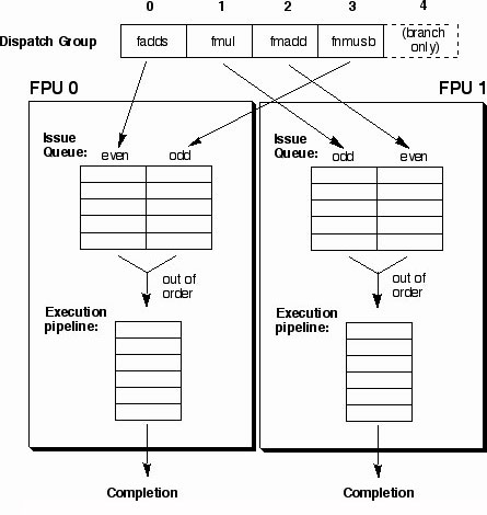
On the G5, each FPU has its own issue queue. The 18 entry queues are divided into halves to hold the instructions that come from even or odd slots in the dispatch group. Dispatch group entries 0 and 3 go to FPU 0. Dispatch group entries 1 and 2 go to FPU 1. Instructions are pulled out of order from the issue queue to fill the execution unit pipeline, with preference to the oldest instructions first. One instruction per cycle may move from the issue queue to the execution unit, per FPU. Up to four instructions per cycle may be placed in the issue queues.
Because of this partitioning scheme, it is possible (although unlikely) for poorly scheduled code to utilize exclusively one of the two FPUs. Likewise, if you only use dispatch group slots 0 and 2 for FPU instruction (with 1 and 3 for loads, for example) then you will only have 5 of the 10 issue queue slots available used each FPU. This is because you will only be using the even half of each.
To help make sure the processor is not data starved, the G5 provides two load/store units to support your work. (Earlier PowerPC processors have one.) The way instructions flow through the LSUs is very similar to the FPUs. The LSU issue queues are shared with the two integer units. One integer and one LSU operation can be issued from each LSU/FXU queue per cycle. Load latencies for the FPUs are a bit longer than for the integer units.
The double precision floating point functionality in vecLib.framework has been retuned for G5 for MacOS X.2.7 and later. Additional performance enhancements, especially to matrix multiplication in the BLAS, are available in MacOS X.3, Panther.
Writing G5 specific code
Generally speaking, it is a mistake to tie specific software features to certain processors. Doing so is necessarily fragile because as new processors come out your code will not grow to take advantage of them. In certain cases, G5 specific code might be required to work correctly on the next processor as well. One example might be using dcbz, for which the size of the cacheline is critical. Code that assumes that only G5 has a 128 byte cacheline, and all others are 32 bytes will fail if another processor arrives that no longer calls itself a G5, but which has 128 byte cacheline size.
Instead, Apple recommends that you tie your code to specific processor features. This way as new processors are introduced, your code will dynamically adjust to do the right thing. MacOS X.3, Panther, introduces a new API to replace sysctl, called sysctlbyname, which has been enhanced to return 64 bit results for key items like processor frequency that no longer fit in 32 bits or are unlikely to do so in the near future. There are a number of keys available to determine if various processor features are available.
Here is sample code for determining the number of bytes in a cacheline:
#include <sys/sysctl.h>
//Returns the size of the cacheline in bytes

									size_t GetCachelineSize( void )

									{
const char key[] = "hw.cachelinesize";

										u_int64_t result = 0;

										size_t typeSize = sizeof( result );
int err = sysctlbyname( key, &result, &typeSize, NULL, 0 );

										if( 0 != err )  return 0;
return result;
}
A great many other selectors are available. For more information, please see the sysctlbyname man page and /usr/include/sys/sysctl.h.
Using the PowerPC 970 Cycle Accurate Simulator
The G5 core is much more complicated than the G4. A cycle accurate simulator is a must to truly understanding the roots of code performance on G5. While certainly not required to optimize every piece of code, some time spent with the G5 simulator is almost always a well spent learning experience that should help you anticipate and avoid performance pitfalls. Apple provides such a simulator in the form of simg5, available with CHUD 3.0.1 or better.
To use SimG5, the first thing you have to do is collect a trace as per what you would do for SimG4. On MacOS X, this is done using amber. We mostly use a supervisor level instruction as a trigger and collect the next 5000 instructions afterwards. The trigger toggles sample collection on and off. Other approaches work fine too, but many of them may lead to huge traces of stuff you don't want to see.
To insert a supervisor level instruction, add this one line where you want to start tracing:
#if defined( __GNUC__ )

									#include <ppc_intrinsics.h>

									#endif
int myTempVariable = __mfspr( 1023 );
...and then recompile with GCC or MWCW. (Other compilers may not recognize __mfspr() and may require other syntax to introduce that instruction.) This will cause your program to crash when it hits that instruction. Run the program under amber however, and it will intercept the exception and start tracing at that point.
CHUD 3.0.1 and later users may instead elect to use the following function call to start or stop a trace at a specific point:
void chudStartStopAmber(void);
If your app is called a.out, you can collect a trace of 5000 instructions after the supervisor level instruction from the command line as follows:
amber -x 5000 -I ./a.out
If you have a Cocoa app, navigate down to myApp.app/Contents/MacOS/ where you will find the actual executable for the app, and use that in place of a.out above. If you have a CFM app, then you need to run your app through LaunchCFMApp through amber:
/usr/bin/amber -x 5000 -I /System/Library/Frameworks/Carbon.framework/Versions/A/Support/LaunchCFMApp ./a.out
Set up some aliases and things will be simpler. You can collect a trace on a G4 if you like. A G5 is not required.
When amber is done, it should produce a directory called trace_001, and inside you will find a file called thread_001.tt6e, that contains information on what instructions were issued in what order and some additional information like addresses for loads and stores. So far, everything in this procedure has been the same as what you'd do to collect a trace for SimG4.
Once you have the trace in hand, you can run the simulator as follows from the terminal:
simg5 thread_001.tt6e 5000 100 1 simg5 -p 1 -b 1 -e 5000
This will produce two files, simg5.pipe and simg5.config that contain the simulator output. When running simg5, you may find a few other options handy, especially the -inf* options for turning off things like cache misses. These can be distracting if your code spends most of its time in load stalls.
-inf_L1 |
- make the I and D side L1 caches infinite. | |
-inf_tlb |
- make the I and D side TLB's infinite. | |
-inf_translate |
- all ops will always pass translation. | |
-inf_L2 |
- make the L2 infinite. | |
-inf_store |
- don't send stores to the L2 (for use with inf_L1). |
The output files can be visualized with the java viewer as follows:
scrollpv -pipe simg5.pipe -config simg5.config
Please be aware that this process is not all that speedy, so give it a minute or two to appear. 5000 instructions is actually quite a lot for this java app. When the java viewer comes up, the first thing you will want to do is turn on autoscroll based on F: Select Symbol tracking from the Scroll Mode menu in the window. Enable Track on F with offset of 0. This will help keep the interesting region in the window as you move the vertical scroll bar. SimG5 doesn't wrap the way SimG4 did. This can also be done by double clicking on F.
You'll see something that looks like the SimG4 horizontal scroll pipe. You can mouse over the various symbols in the window and the viewer will tell you what they mean.
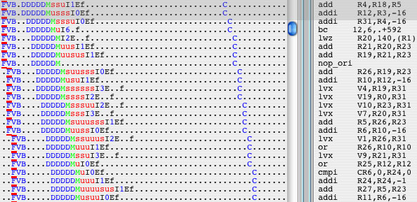
Each column is a cpu cycle. Each row is an instruction. As you read along a row from left to right you can see that instruction progress through the processor. You can see the dispatch groups of four as sets of four instructions that begin dispatch/decode (DDDDDM) and enter completion (C) together. As described above, the instruction first is fetched (FVB) into the instruction buffer. Then there is a delay for some number of cycles before the dispatch mechanism reaches those instructions and forms a dispatch group out of them. They go through 5 cycles of decode (DDDDD) and one of dispatch (M). At that point they are sitting in the issue queues in front of each execution unit. There they may reside for a few (or a great many) cycles (su) until the resources they need become available for them to issue into the execution units. You can see that instructions can be reordered within these queues. For example, the add that appears right after the noop actually enters execution after an addi that appears seven instructions later. Which execution unit they issue into is given by the number that follows the (I). Move the mouse over it to find out which one it is. Once the instructions are in the execution unit, they execute for a while and then finish (f). Finally, there is a delay while the CPU waits for all instructions in a dispatch group to finish and the group before it to finish, before the group can complete (C). Dispatch groups must complete in the order that they were dispatched.
The simg5 simulator and scrollpv viewer are available from Apple in CHUD 3.0.1 and later.
|
Get information on Apple products. Copyright © 2008 Apple Computer, Inc. |