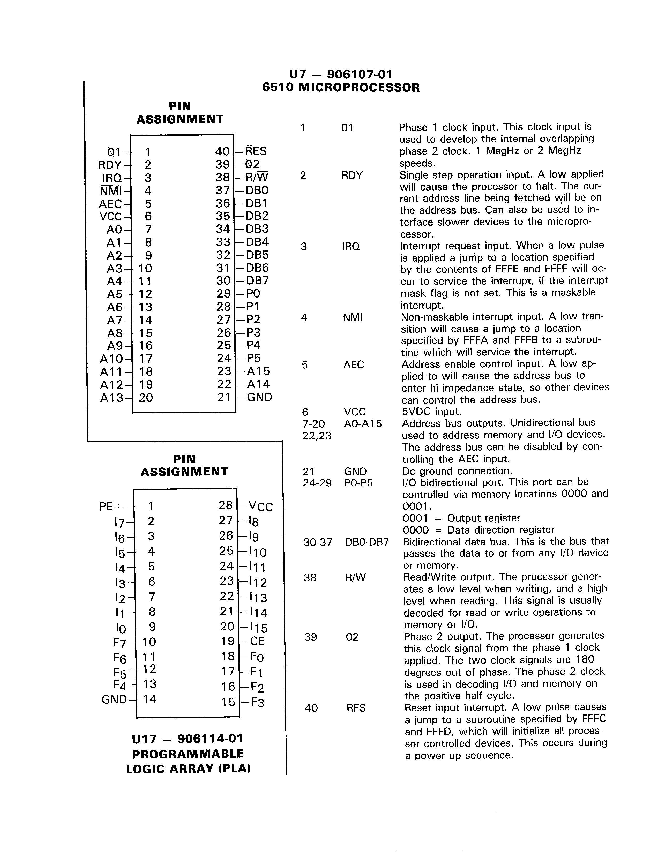
ocr: U7 - 906107-01 6510 MICROPROCESSOR PIN ASSIGNMENT 1 01 Phase 1 clock input. This clock input is used to develop the internal overlapping Q1 1 40 -RES phase 2 clock. 1 MegHz or 2 MegHz RDY 2 39 - Q2 speeds. IRO 3 38 R/W 2 RDY Single step operation input. A low applied NMI 4 37 DBO will cause the processor to fetched halt. will The be cur- on AEC VCC 5 6 7 35 34 36 - - - DB1 DB2 DB3 the rent tertace cessor. address address slower bus. line devices Can being also to the be used micropro- to in- AO A1 8 33 -DB4 3 IRQ Interrupt request input. When a low pulse A2- 9 32 - -DB5 is applied a jump to a ...