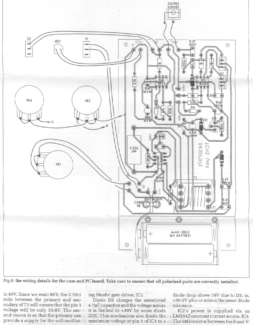
Labels:text | sketch | diagram | drawing | technical drawing | plan | schematic OCR: OUTPUT SOCKET 10 S LED 103J TUD 0.47 100V 11 - 02 1500 IC2 555 D2 A153 10ul 16VW ₡ 2.21 B 18k 0.33 VR4 VR3 05 120 10uF D4 25VM 100k JouF ZD1 D3 680 4.7 GF ABS 63VW .001 ДЕИ2 nU!+ 0.220 5W 0081 VR 100UF TI 16VW 100VW ( -) BLACK CABLE RED 0.47 TIE 1001 O O + 4xAA CELLS (6V BATTERY] 0 Fig.8: the wiring details for the case and PC board. Take care to ensure that all polarised parts are correctly installed. is 40V. Since we want 80V, the 2.59:1 ing Mosfet gate driver, IC2. ratio between the primary and sec- ondary of T1 will ensure that the pin 1 Diode D3 charges the associated diode drop above 39V due to D3; ie, +39.6V plus or minus the zener diode voltage will be only 30.9V. The sec- 4.7UF capacitor and the voltage across tolerance. it is limited to +39V by zener diode ond reason is so that t ...