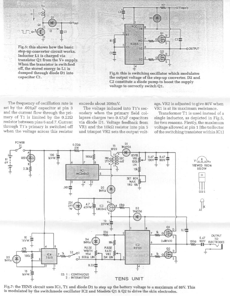
Labels:text | diagram | plan | technical drawing | schematic | black and white | parallel OCR: RZ -OVsupply C3 OVOUT VCC ZLOB VB 12 -CI RT D HO R2155 Fig.5: this shows how the basic CT step-up converter circuit works. VS OOUTPUT 02: Inductor L1 is charged via D transistor Q1 from the V+ supply. LO 5 When the transistor is switched off, the stored energy in L1 is dumped through diode D1 into capacitor C1. Fig.6: this is switching oscillator which modulates the output voltage of the step-up converter. D2 and C2 constitute a diode pump to boost the supply voltage to correctly switch Q1. The frequency of oscillation rate is set by the .001uF capacitor at pin 3 exceeds about 300mV. age. VR2 is adjusted to give 80V when The voltage induced into T1's sec- VR1 is at its maximum resistance. and the current flow through the pri- mary of T1 is limited by the 0.220 ondary when the primary field ...