home
***
CD-ROM
|
disk
|
FTP
|
other
***
search
/
c64.rulez.org
/
2014.05.c64.rulez.org.tar
/
c64.rulez.org
/
pub
/
plus4
/
Docs
/
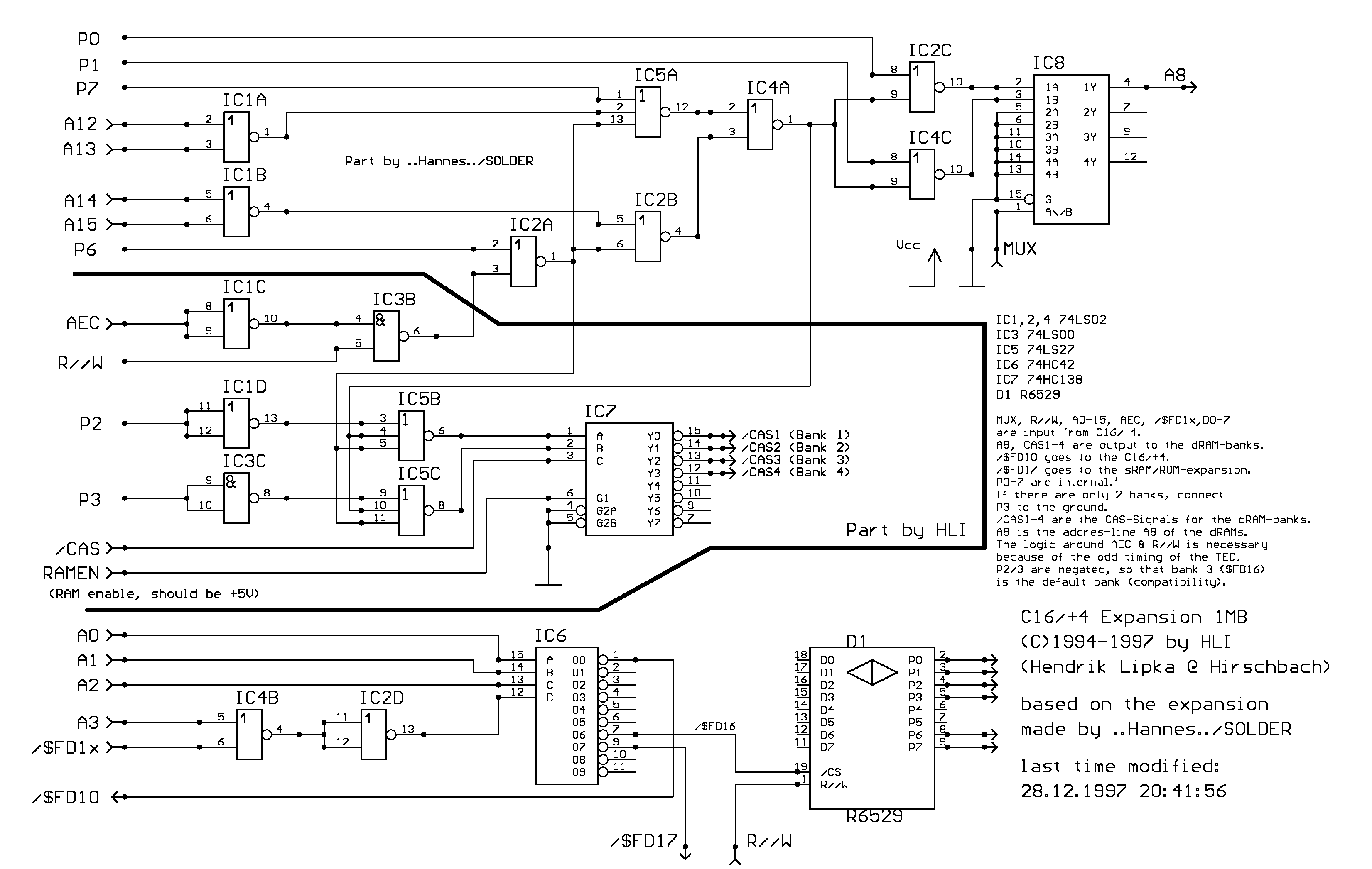
1_Meg_Expansion.gif
next >
Graphics Interchange Format
|
2005-11-30
|
95KB
|
3303x2094
Labels:
diagram
|
text
|
technical drawing
|
plan
|
schematic
|
sketch
|
black and white
OCR:
PO IC2C P1 1 PZ IC5A 8 IC8 IC4A A8 10 2 1 9 3 1A 1Y 4 IC1A 1 2 12 2 1 5 1B 0 A12>* 2 1 13 2A 2Y 7 1 6 1 3 2B A13 >· 3 IC4C 11 9 10 3A 3Y Part by .. Hannes .. /SOLDER 8 1 14 3B 4A 44 12 IC1B 10 13 9 4B A14>. 5 1 IC2B 15 4 G 1 A15 >. 6 IC2A 5 AV/B 1 4 P6 2 1 6 Vcc · MUX 1 1 3 IC1C IC3B 8 1 AEC >* 10 4 IC1,2,4 74LS02 9 IC3 74LSOO 5 R//W IC5 74LS27 . IC6 74HC42 IC1D IC7 74HC138 IC5B D1 R6529 11 1 P2 . IC7 3 1 MUX, R//W, A0-15, AEC, /$FD1x, DO-7 12 13 4 6 1 15 /CAS1 (Bank 1) are input from C16/+4. () 5 2 A YO B Y1 14 /CAS2 (Bank 13 2> A8, CAS1-4 are output to the dRAM-banks. IC3C 3 C Y2 /CAS3 (Bank 3) /SFD10 goes to the C16/+4. IC5C Y3 12 /CAS4 (Bank 4> /SFD17 goes to the SRAM/ROM-expansion. 9 11 PO-7 are internal.' P3 . 8 9 Y4 6 10 If there are only 2 banks, connect 10 10 8 4 G1 Y5 Y6 P3 to th ...