 74ls17574f175
quad d-type flip-flop
74ls17574f175pin assignment |
logic diagram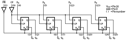 |
|
h = high VOLTAGE LEVEL STEADY STATE. H = high VOLTAGE LEVEL ONE SETUP TIME PRIOR TO THE low-TO-high CLOCK TRANSITION. l = low VOLTAGE LEVEL STEADY STATE. L = low VOLTAGE LEVEL ONE SETUP TIME PRIOR TO THE low-TO-high CLOCK TRANSITION.  = low-TO-high CLOCK TRANSITION. = low-TO-high CLOCK TRANSITION.x = DON'T CARE. |
||||||||||||||||||
74f241pin assignment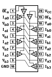 |
logic diagram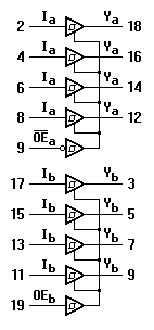 |
h = high VOLTAGE LEVEL l = low VOLTAGE LEVEL x = dON'T CARE (z) = high IMPEDANCE (OFF) STATE | ||||||||||||||||||
pin assignment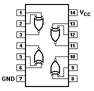 |
logic diagram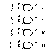
|
h = high VOLTAGE LEVEL l = low VOLTAGE LEVEL |
|||||||||

